澳門的微電子集成電路片設計技術
Rui Martins① 龐志偉②]
L.W.Tim,U.S.Pan③
(澳門大學科技學院)
摘要
本文叙述了1994年上半年在澳門大學科技學院所進行的一個科研項目的成果。該項目設計了具有1.2微米CMOS技術(來自澳地利的Austria Mikro Systeme AMS)的集成電路,是與葡萄牙里斯本高級工程學院(IST)的集成電路與系統研究組共同合作的。設計工作是由澳門大學科技學院的電機與電子工程的碩士研究生們學習微電子電路設計課程時所作的設計。10個學生設計了具有以下功能的基本電路:開關電容雙型濾波器,4位數/模轉模器,16位靜態RAM和16位動態RAM,4狀態波形發生器和4位/7段顯示解碼器和寄存器。經過仿眞和佈置,這五種電路被綜合在一個多功能版(MPC-在澳門是第一個這樣設計)中,並送交奧地利AMS工廠製造。整個版的硅片面積為6mm2,具有48隻腳。本文列出了其様品版的照片和測量結果。
1.Introduction
Growing technological requirements and the widespread acceptance of sophisticated electronic devices have created an unprecedented demand for design and fabrication of very largescale and complex integrated circuits-IC's. The fast development of CMOS technology, with process characteristics allowing the mix in the same chip of digital and analog functions, was the main responsible for the appearance of a wide range of electronic products (for ex. mobile phones, handycam video cameras, etc.)that extensively use the advantages in terms of size and power consumption reduction, allied with high performance, of monolithic IC's.
The main purpose of the project UMCHIP[1]was to motivate, first of all, a group of post-graduate students with diversified preparation in Electronics, for the acquisition of knowledge in terms of the basic electronic principles and techniques needed by the designer throughout the CMOS IC design process. This project was the last part of the evaluation process in a Master course named Microelectronic Circuit Design and it can beconsidered as a whole a very good result because each group of students was able to finish a complete process of calculation and design, computer simulation and layout of a specific function in IC form using an advanced CMOS technology of 1.2μm from AMS (with double poly and double metal layers) [2]. There were even some cases where some of the groups obtained very good testing results on the chip (after fabrication). This aspect is of significant importance because in the beginning of the course the knowledge about CMOS IC design was almost none (regardless of the fact that the students came from different Universities, either in China, Hong Kong and Macau) and the duration of the course (4 months part-time) associated with the duration of the design procedures (1.5 months also in a part-time basis) was too short to achieve a good result in a first prototype. Nevertheless, the final architecture of the chip in terms of area (less than 6mm2) is quite reasonable for the different Analog and Digital-A/D functions implemented: SC Biquad Fiter, 4-bits D/A Converter, 16-bits SRAM & 16-bits DRAM, 4-Phases Waveform Generator, 4-bits/7 segments Display plus a Super-buffer. These functions were chosen because they constitute some of the most important functions that can be found in a high variety of IC's with applications in Telecommunication and Control Systems. The testing results obtained with the prototype samples can also be considered satisfactory for a first run of a mixed A/D circuit.
In this paper, we will present for the different projects included in this MPC the architectures, simulation results (electronic simulation-with HSPICE program [3]) layout (with MAGIC program [4]) and also some results obtained with the firstprototype chip. In Section 2 we will present the design and simulation results of a Switched-Capacitor Biquad Lowpass Notch Filter, including a functional simulation of the architecture with SWITCAP-2 program [5] and electronic simulations of a CMOS Class AB-Operational Amplifter-OA. In Section 3, we will present the architecture, simulation results and the layout of a 4bits D/A Converter using a charge re-distribution architecture that includes a class A OA. In Section 4 a 16-bits DRAM and a 16-bits SRAM, including decoding logic are presented in terms of the architectures, design simulations and layout. In Section 5, we present a Multiphase Switching Waveform Generator (based on D-type Flip-Flops) capable of controlling the SC Biquad Filter of section 2. In Section 6 a Programmable Logic Array - PLA that implements a 4-bits (BCD)/7 segments display decoder is presented together with a digital Super-buffer, including measured results obtained with the first prototype samples. Finally, in Section 7 we will present the Microphotograph of the Chip and the Conclusions.
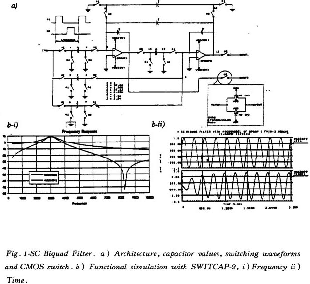
2.Switched-Capacitor Biquad Filter
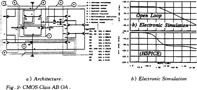
The SC Biquad Filter designed in the section is a Lowpass Notch Filter with a complex pair of poles @ fp=3.08kHz with Qp = 3.9 and a notch @ fN = 8. 15kHz, being the sampling frequency Fs = 384kHz [6]. This SC filter can be used as part of a more complex filtering structure used in the reception path of the analog interface of a 9.6kHz modem. The architecture of the Biquad is presented in Fig. 1-a), together with the capacitorvalues, the 2 non-overlapping clock waveforms and the electronic structure of a CMOS switch. In Fig. 1-b) we present results of the functional simulation using SWITCAP-2. In Fig. 2 we present the structure of the class AB OA designed with a Gain = 70 dB and GBW = 10 MHz (>10 Fs).
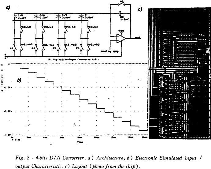
3.4-bits Digital/Analog Converter
The architecture of an inverting 4-bits charge redistribution D/A Converter is presented in Fig. 3-a). During the reset phase (p1), the binary-weighted capacitor array and the capacitor 2C around the OA are discharged through the virtual ground. During the conversion (or set) phase, under the control of the input binary digital code, part of the array is connected to the reference voltage (V ref), thus injecting a charge into the virtual ground which will be integrated by 2C. Assuming that the binary-weighted capacitor array can be written as Cbi= (1/2)i-1 .C (with i = 1, 2, …4) and considering the charge conservation principle, we can write during the conversion (or set) phase the following equation
Vo=-Vref.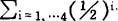 bi
bi
that reflects the behavior of the D/A converter. The electronic simulated input / output characteristic of this converter (based on the above equation), obtained by HSPICE (considering a CMOS class A OA) is presented in Fig. 3-b) [7]. In the Fig. 3-c) we present the layout architecture where we can clearly see the OA (top) and the capactior array (bottom right).
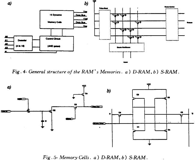
4.16-bits Dynamic-RAM and 16-bits Static-RAM
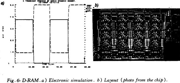
The 16-bits D-RAM and 16-bits S-RAM presented in this section have the general structure shown in Fig. 4-a) and 4-b), respectively[8]. On the other hand, the basic D-RAM and SRAM cells, are presented in Fig. 5-a) and Fig. 5-b). In Fig. 6-a) is presented the transient process of the read cycle in the D = RAM (as obtained from a simulation with HSPICE) and in Fig. 6-b) we can see the layout of the D-RAM and the logic decoder.
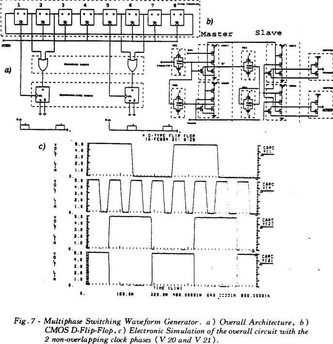
5.Multiphase Switching Waveform Generator
A Multiphase Switching Waveform Generator was designed to meet the necessary requirements of the 2 non-overlapping clock phases that will control the SC Biquad Filter presented before. The architecture used for the Generator is based on a Ring Counter and is presented in Fig. 7-a), being the basic cell constituted by a Master/Slave D-Flip Flop (Fig.7-b)). On the other hand in the Fig. 7-c) we present an electronic simulation where we can clearly see the two non-overlapping phases (V 20 and V 21) [9].
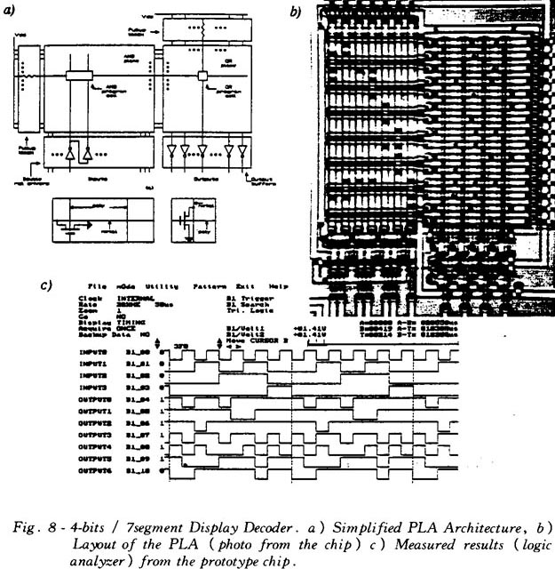
6.4-bits(BCD)/7 segments display PLA Decoder plus a Super-buffer(includes Measured Results)
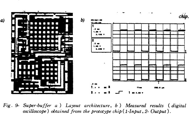
A PLA is usually constituted by two major subsections or planes as presented in Fig.8-a). The AND plane requires double rail inputs (each independent variable and its complement) to generate the product terms required by the defining logic equations of a 4-bits / 7 segments decoder [10]. The OR plane will make the logic adition (OR) of the different product terms to produce the dependent variables [10]. In Fig.8-b) we present the overall layout of the PLA decoder (as obtained from a photo of the chip) where we can clearly see the AND plane (right sidewith 4 inputs) and the OR plane (left side-with 7 outputs). In Fig.8-c) a measured result extracted from the operation of the chip (by means of a logic analyzer) is presented, where we can see the different input configurations (BCD) and the resulting outputs that switch on or off the 7 segments of a led display. It was also designed a Super-buffer that is presented in terms of layout in Fig. 9-a), with measured results (obtained in a digital oscilloscope) show in Fig. 9-b).
7.UMCHIP Microphotograph and Conclusions
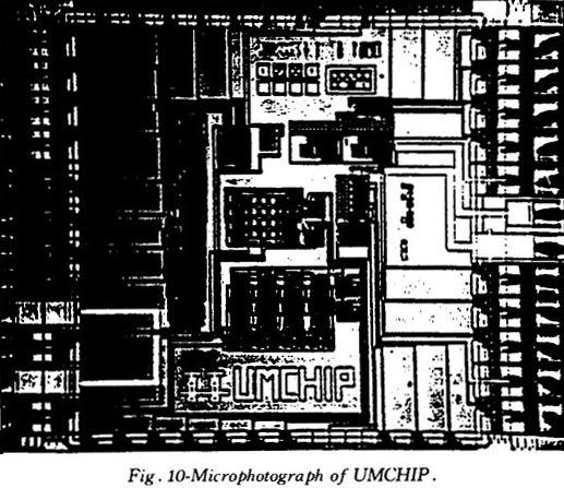
The microphotograph of the overall UMCHIP is presented in the Fig. 10, occupying a total area of 6mm>2. As a conclusion we can say that, this paper presented, with good results, the first Integrated Circuit designed in Macau. This was only possible with the big effort developed by the 10 Master students in Electrical and Electronics Engineering, referred as authors, that were able in a short period of time to learn the necessary fundamental knowledge about CMOS IC design in order to finish the complete design procedure of 5 basic analog or digital functions involving simulation, layout and testing of the chip prototype samples. The measured results obtained can beconsidered satisfactory for a first run of a mixed analog-digital circuit.
Acknowledgements: We would like to thank the Research Committee of the University of Macau and Macau Foundation for the financial support and the Integrated Circuits and Systems Group of Instituto Superior Técnico for the technical support.
①副敎授(來自葡萄牙IST)
②研究助理科技學院畢業生。
③碩士研究生
References
(1) “UMCHIP-University of Macau CHIP”, Project Proposal approved by the Research Committee of Univ. Macau, Faculty of Science and Tecnology, University of Macau, Macau, November 1993.
(2) “Austria Mikro Systeme-AMS”, Design Rules and TargetIntrinsic Parameters for the CAB/CAE 1. 2 μm CMOS Technology, Graz, 1993.
(3)“HSPICE”, User's Manual Meta-Software, Inc., 1990.
(4)“MAGIC”, User's Manual-Version 6, University of California @ Berkeley,1990.
(5)K. Suyama, S. C. Fang. “SWITCAP 2” - User's Manual Version 1.1 Columbia University, 1992.
(6) U Seng Pan, Chou On Sek, Switched-Capacitor Filter (SC Biquad), Final Project Report, Microelectronic Circuit Design, Faculty of Science and Tecnology, University of Macau, Macau, March 1994.
(7)Tam Kin Seng, Leong Cheok Teng, Digital-Analogue Converter (Charge Re-distribution), Final Project Report.Microelectronic Circuit Design, Faculty of Science and Tecnology, University of Macau. Macau, February 1994.
(8)Cheang Tak Son, Wong Man Chung, Memory Cells (DRAM + SRAM), Final Project Report, Microelectronic Circuit Design, Fac. of Sience and Tecnology, University of Macau,Macau, March 1994.
(9)Lo Wa Kit, Wong Chi Kong, Multiphase Switching Waveform Generator (with D-type Filp-Flops, NOR Gates, Inverters), Final Project Report, Microelectronic Circuit Design, Faculty of Science and Tecnology, University of Macau, Macau, March 1994.
(10)Lou Weng Tim, Mak Peng King, PLA (BCD - 7 segments decoder), Final Project Report, Microelectronic Circuit Design Faculty of Science and Tecnology, University of Macau, Macau, February 1994.